 See Vivado™ Development Environment on amd.com
|
- Introduction
- Basic Versal Design using Vivado IP integrator
- Step 1: Project Creation
- Step 2: Initial CIPS, NoC & DDR-MC Instantiation with Block Automation
- Step 3: CIPS Customization
- Step 4: Referencing RTL Modules
- Step 5: Adding RTL as Packaged IP
- Step 6: Design Validation
- Step 7: Generate HDL Wrapper, Constraints, Synthesis
- Step 8: Advanced I/O Planner
- Step 9: Implementation, Generating Device Image
Version: Vivado 2022.1
When using a Versal device, the IP integrator creates a Block Design (BD) that contains a CIPS block (Control, Interfaces & Processing System) and the NoC (Network-On-Chip) with DDR-MC (DDR Memory Controller).
An AXI-based RTL module will be imported using IP integrator Module Reference to demonstrate how users can quickly add their own RTL to a block design. A second RTL based IP that is packaged as an IP repository will also be added to the Block Design.
The IP integrator Designer Assistance is also featured in this tutorial to perform Block and Connection Automation to assist in the creation of module blocks and the connect of these modules. Once the design is validated and the RTL wrapper is created, initial constraints are then added before running RTL synthesis. After synthesis is complete, the “Advanced IO Planner” is used to constrain the DDR-MC pinout prior to running implementation and finally generating the device image.
Highlighted steps include:
-
Vivado Project Creation
-
CIPS Instantiation and Configuration
-
NoC and DDR-MC Creation using Block Automation
-
RTL IP by Module Reference and connectivity with Connection Automation
-
RTL IP using IP repository
-
Final Validation
-
RTL Wrapper Generation
-
Initial Constraints
-
Synthesis
-
Advanced IO Planner constraints
-
Implementation
-
Generate Device Image
-
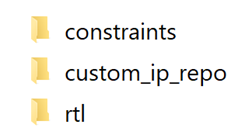
Unzip the tutorial .zip file. It should create the following sub-directories in a working area:
Note: If using Windows, unzip to C:/ to avoid the 256-character directory limit.
-
Invoke Vivado 2022.1 IDE GUI.
-
In the GUI go to Quick Start and select “Create Project”. Keep the default project name “project_1”. Set the project location to a working directory for the project. The “project_1” directory should be created at the same directory level as the files shown in step 1.
-
Click through the following menus accepting default settings which should be:
-
Project Type: RTL Project
-
Add Sources: (leave blank)
-
Add Constraints: (leave blank)
-
-
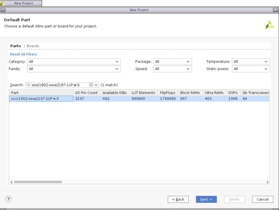
In the “Default Part” menu, select the following Versal AI device:
-
xcvc1902-vsva2197-1LP-e-S
-
click “Next”
-
-
On the next menu, review the “New Project Summary”. If everything looks correct, click “Finish”

The CIPS block will be instantiated on the Block Design IP integrator canvas and with the use of IP integrator “Block Automation”, the NoC and DDR-MC modules will be initially configured and instantiated on the IP integrator Canvas. Further customization will be performed after this initial setup.
-
To create a Block Design, click the following in the Flow Navigator pane:
“Project Manager > IP INTEGRATOR > Create Block Design”
Accept the defaults on the pop-up window and click “OK”
-
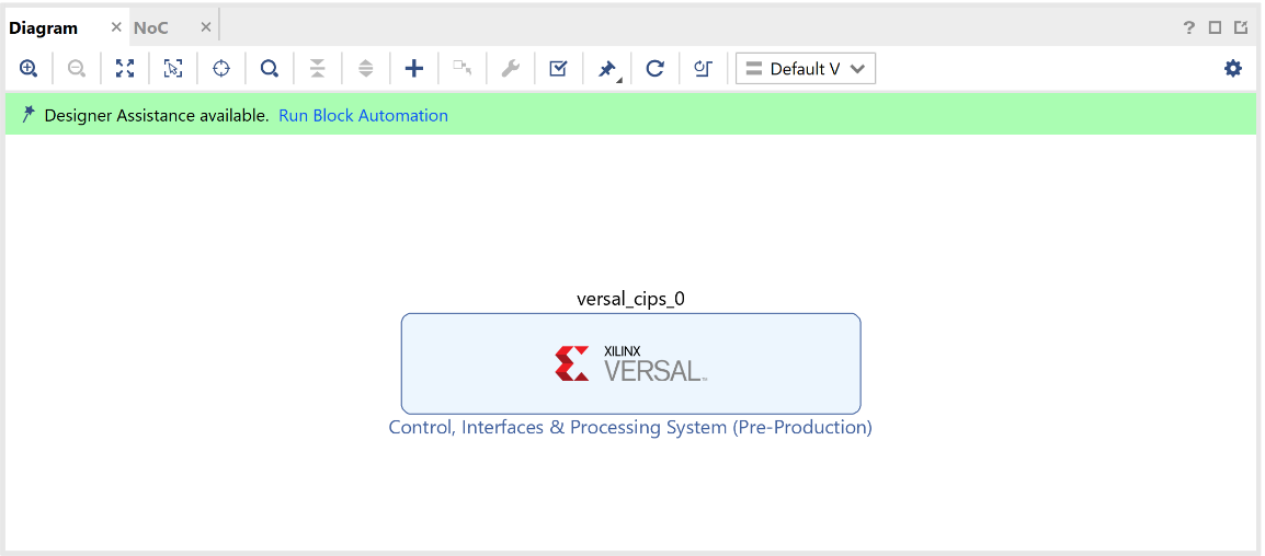
Right click in the IP integrator Canvas and select “Add IP…” and search for “cips”. Double Click on “Control, Interfaces & Processing System” to select and instantiate the CIPS on the IP integrator Canvas. The Versal CIPS module should now appear on the IP integrator Canvas.

-
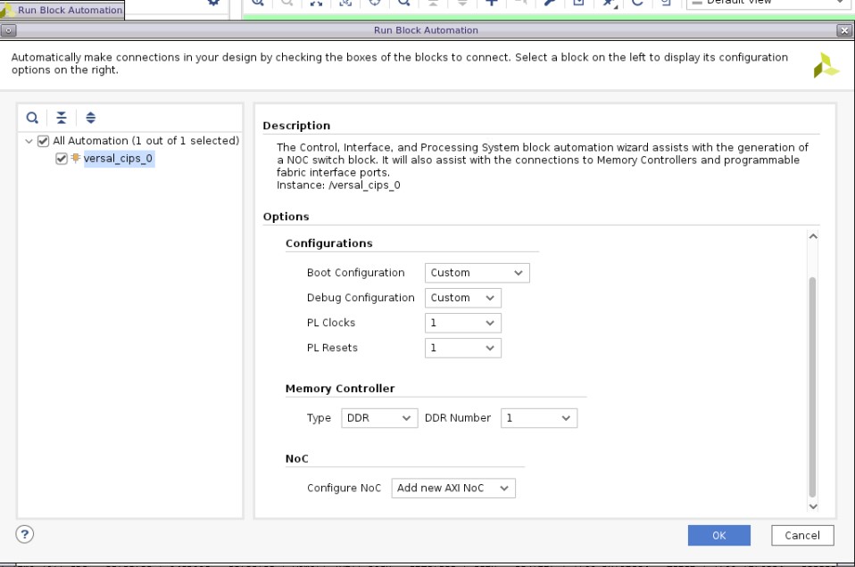
Click on “Run Block Automation” to bring up the block automation menu which allows a user to select configurations of other related blocks. Select a single DDR4 Memory controller and additionally, a single PL reset and PL clock. This reset and clock will be used later by an RTL module. Under Options, change the following settings below, and leave the rest to default.
-
Set PL Clocks to 1
-
Set PL Resets to 1
-
Set Memory Controller (DDR4) to 1
-
-
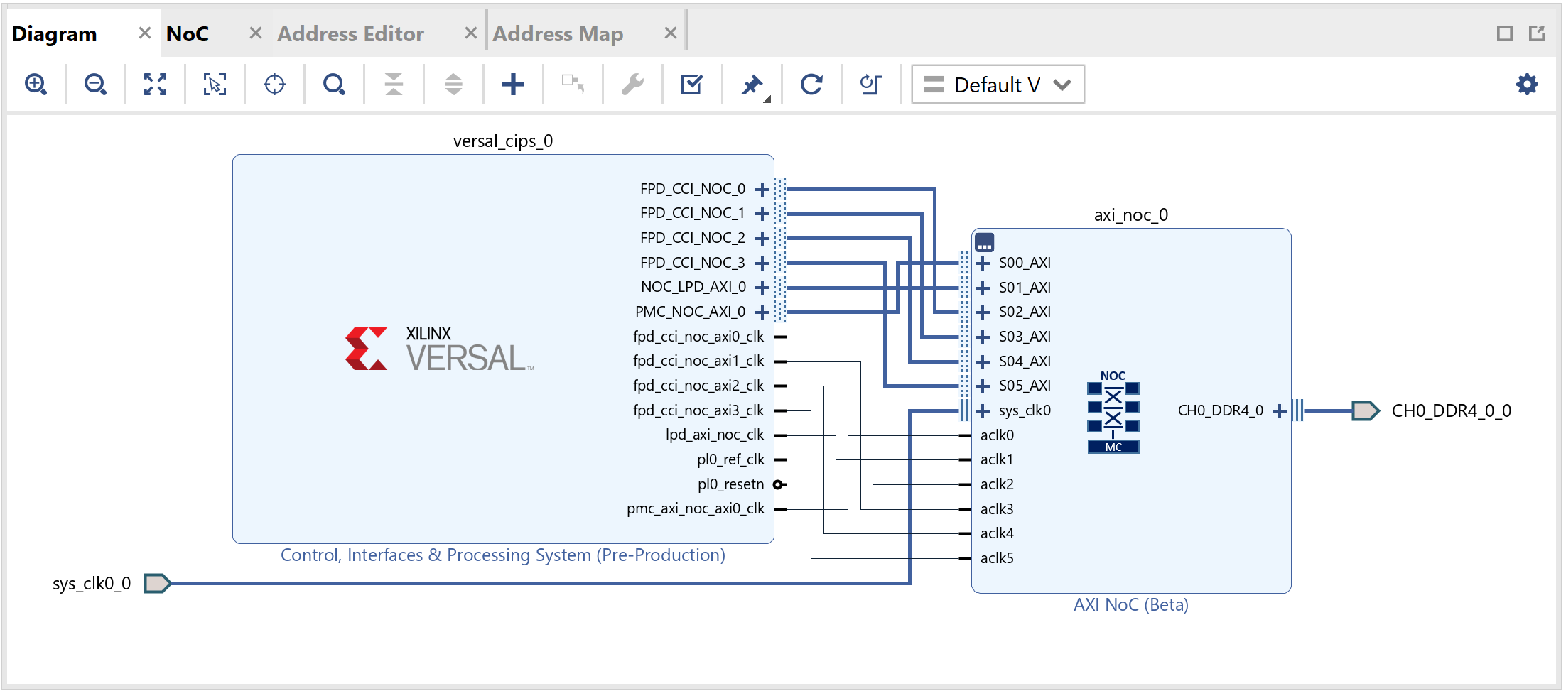
Once the “Block Automation” process is complete, the AXI NoC will now appear on the IP integrator Canvas configured for DDR4 (the DDR-MC is part of the NoC instance) with an external port named “CH0_DDR_0_0” and connections to the CIPS via multiple AXI ports along with associated AXI clock ports with an external clock port named “sys_clk0_0”:
Next, the CIPS will be customized for QSPI and SD Card Boot Modes. We will also configure the PL clock for 200 MHz.
-
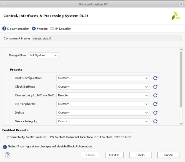
Double-click on the CIPS block to enter the configuration settings for the CIPS. You will see different preset options. Leave them to their default settings and Click Next.
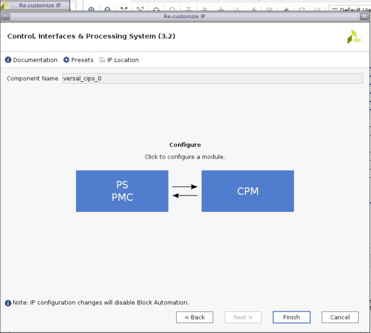
Select PS PMC (click) to change the QSPI and other settings.
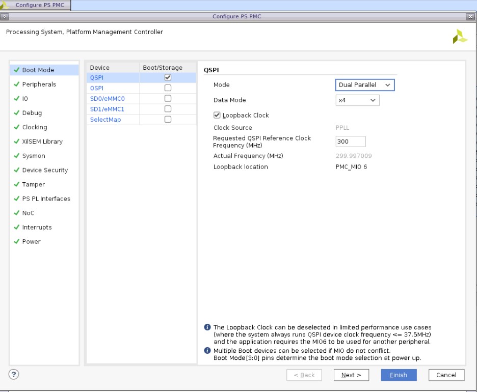
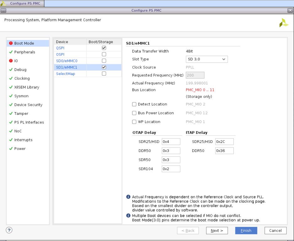
Under Boot Mode make the following changes-
-
Check QSPI
-
Mode: Dual Parallel
-
Data Mode: x4
-
Check Loop Back Clock IO and you can see that the loopback location is set as PMC MIO 6.
-
Under SD 1 / eMCC 1 select the following:
-
Check “SD1”
-
Check Slot Type as SD 3.0.
Note: The default pin location for SD1 is set to PMC MIO 0 ..11 and turns red because it is not available for selection. This is due to some of the pins within the available pin-set getting blocked from use since they were consumed by the prior configured QSPI interface. This can be changed from under the IO tab. Select PMC_MI0 26.. 36 instead of PMC MIO 0 ..11 and the error will be eliminated for this tutorial.
-
-
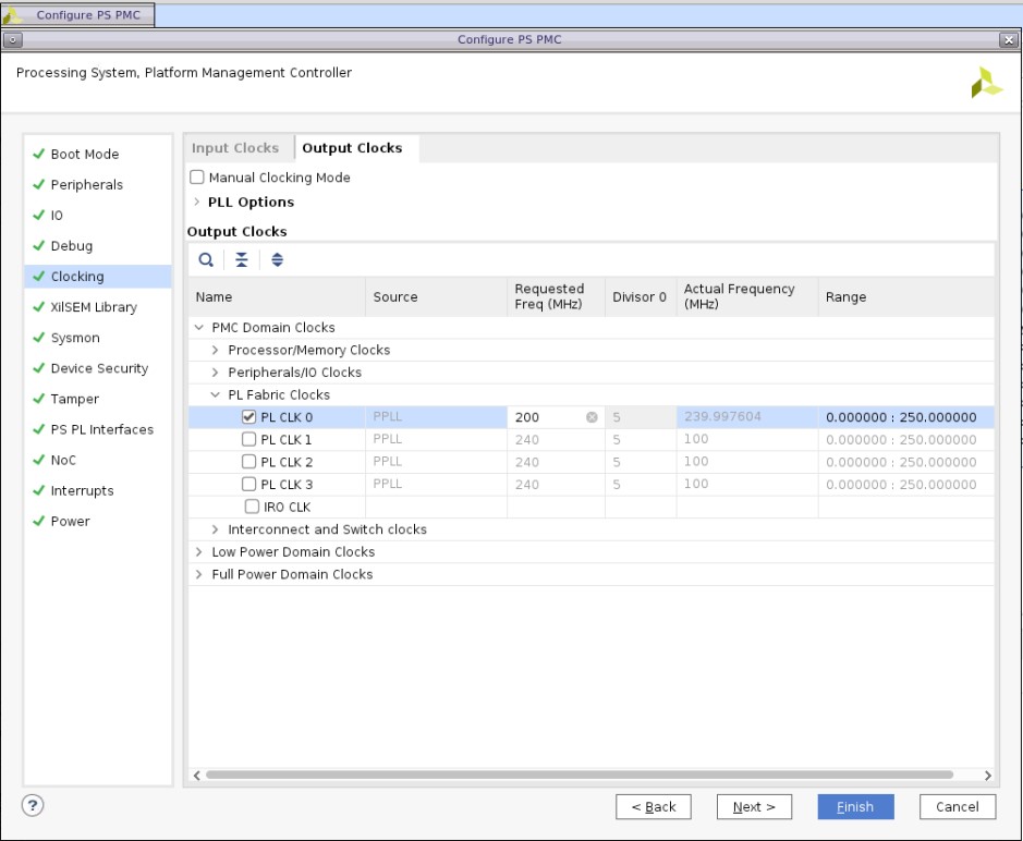
The PL fabric clock needs to be configured for 200 MHz. Under Clocking > Output Clocks > PMC Domain Clocks > PL Fabric Clocks select:
- Check “PL_CLK_0” and set to “200” for 200 MHz (Window columns may have to be moved to view full naming)
Note: The “Actual Frequency (MHz)” differs slightly from the “Requested Frequency (MHz)”. This is due to the accuracy of the PLL that derives this clock for the 33.333 MHz input clock. The input clock is not shown as a port in the BD diagram since it is a dedicated input. It can be observed and changed however in the tab “Configuration Options> PS-PMC > Input Clocks > REF_CLK”
- Click “Finish” to finalize the configuration of the CIPS module.
The Module Reference feature of the Vivado® IP integrator lets you quickly add a module or entity definition from a Verilog or VHDL source file directly into your block design. While this feature does have limitations, it provides a means of quickly adding RTL modules without having to go through the process of packaging the RTL as an IP to be added through the Vivado IP catalog.
Both flows have their benefits and costs:
• The Package IP flow is rigorous and time consuming, but it offers a well-defined IP that can managed through the IP catalog, used in multiple designs, and upgraded as new revisions become available.
• The Module Reference flow is quick, but does not offer the benefits of working through the IP catalog.
Adding a RTL Module by Module Reference
To add HDL to the block design, first you must add the RTL source file to the Vivado project. A PL AXI Slave module called “axi_slave” will now be added to the IP integrator canvas.
-
Add the RTL source “axi_slave.v” provided with the tutorial to the project:
-
“File > Add Sources… > Add or create design sources”
-
“Next” then “Add Files”
-
-
Navigate to the provided tutorial directory and in the “/rtl” directory select “axi_slave.v” and then click “OK” then “Finish”
-
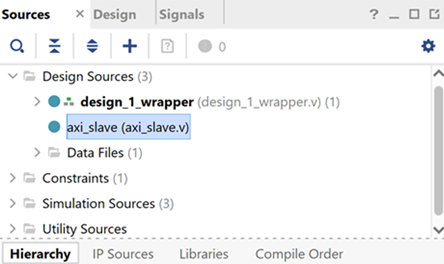
The “axi_slave.v” file should now appear in the “Sources” pane under “Design Sources”. There are a few ways to add the RTL module onto the IP integrator canvas-
- You can click and drag the file onto the IP integrator Canvas.
-
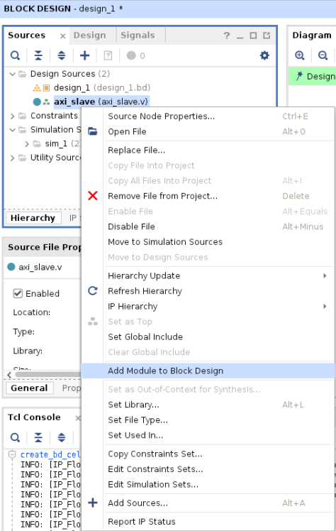
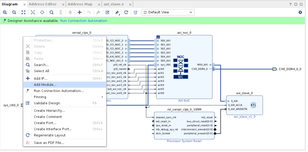
By selecting the module in the Sources window and using the Add Module to Block Design command from the context menu, shown in the following figure.
-
Using the Add Module command from the right-click menu of the design canvas, as shown in the following figure.
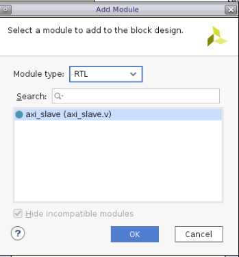
The Add Module dialog box displays a list of all valid modules defined in the RTL source files that you have added to the project. For this tutorial, we have only added the axi_slave module. Select the module to add from the list, and click OK to add it to the block design, shown in the following figure.
-
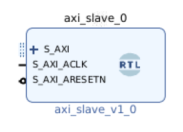
The IP integrator instantiated RTL Module should appear as follows on the IP integrator Canvas:
-
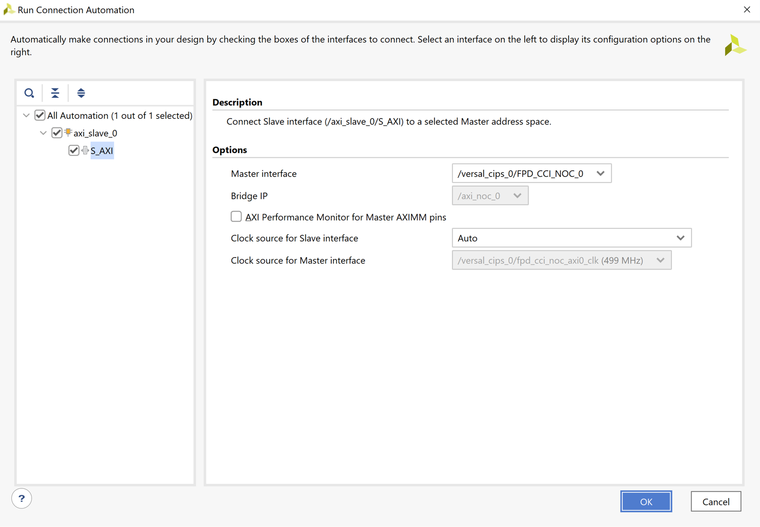
Run “Connection Automation” to connect the AXI port of this module to the NoC:
-
Click “Run Connection Automation” on the top of the IP integrator Canvas
-
Verify that “All Automation” is “checked”
-
Set “Options > Master Interface” to “/versal_cips_0/FPD_CCI_NOC_0” to connect to the CIPS via the NoC
-
Click “OK”
-
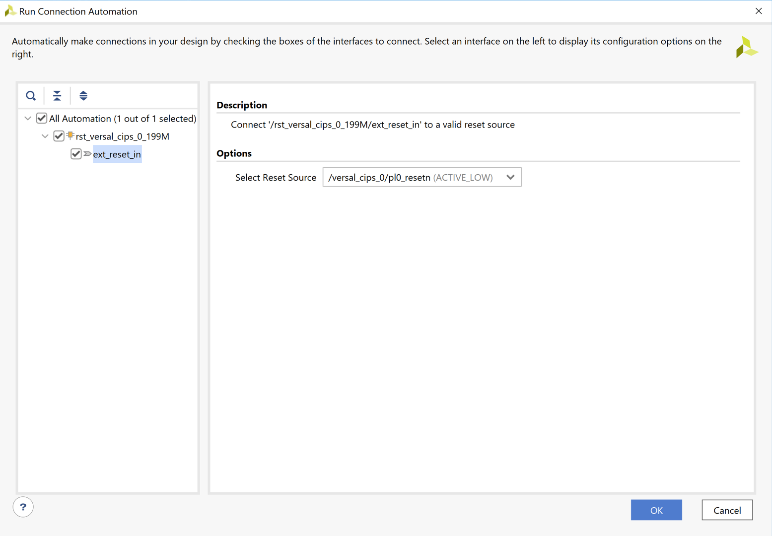
At this point, the RTL module should now be connected to the NoC via AXI and the clock port connected to the CIPS PL clock that was configured earlier. However, the reset on the RTL module is now connected to a “Processor System Reset” module. The input side of the Processor System Reset needs to be connected properly to complete proper connectivity of the reset circuit. Run “Connection Automation” to connect this input to the previously configured CIPS PL reset output.
-
Click “Run Connection Automation” at the top of the IP integrator Canvas.
-
Under “Options > Select Reset Source” select “/versal_cips_0/pl0_resetn”.
- Click “OK”.
-
-
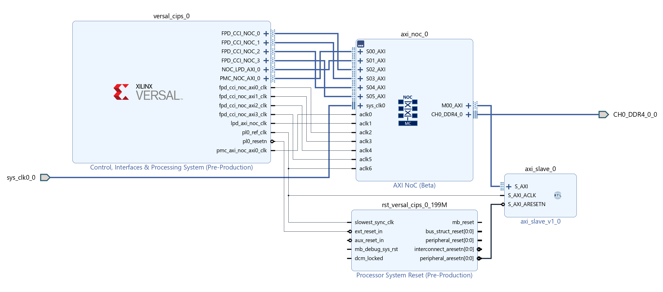
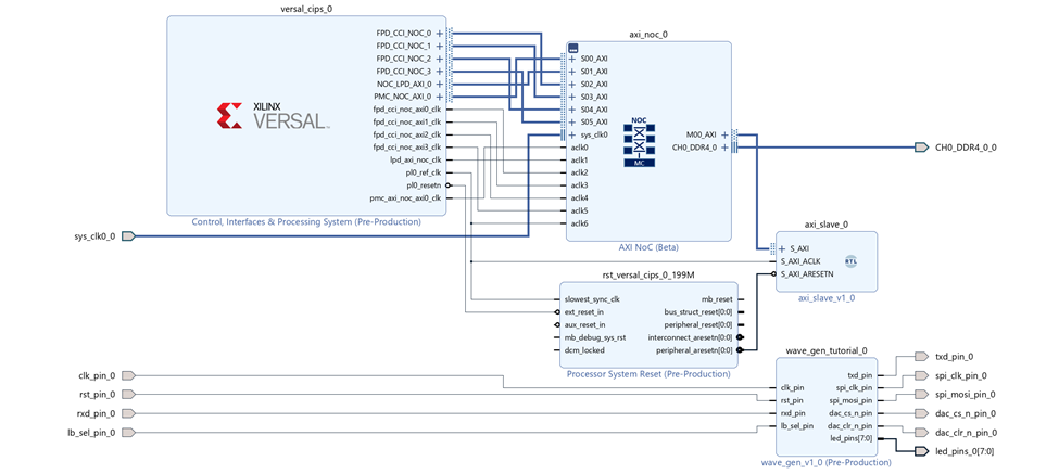
Right click on the IP integrator Canvas and select Regenerate Layout. The Block Diagram should now appear similar-to the following diagram:
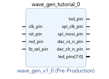
In this section of the tutorial, a non-AXI RTL IP called “wave_gen_v1_0” that has previously been packaged with IP Packager will be added to the IP integrator Canvas with independent external IO connectivity (no connection to CIPS or the NoC). This packaged IP is provided with the tutorial files under the sub-directory “/custom_ip_repo”. Further information on the packaging flow for this IP can be found in UG1119 Lab 4.
-
The IP Repository for the “wave_gen_v1_0” IP must first be added to IP Catalog. First open IP Catalog (IPC):
-
Select “Flow Navigator > Project Manager > IP Catalog”
-
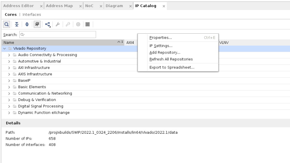
Right Click in IP Catalog pane and select “Add Repository…”
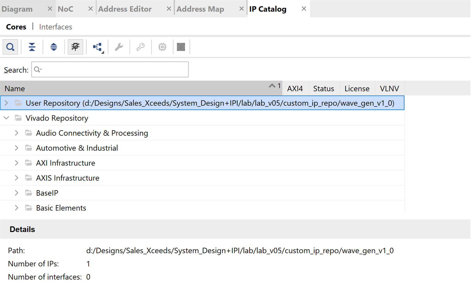
- Navigate to /custom_ip_repo/wave_gen_v1_0” and click “Select” then click “OK”. The added IP should now appear under “User Repository” in IPC:
-
-
Now that the IP Repo has been added to IP Catalog, the IP can be instantiated on the IP integrator Canvas. In the Block Design “Diagram” tab, right click on the IP integrator Canvas and select “Add IP”.
-
In the Search window type “wave” and select “wave_gen_v1_0”. This IP should now appear on the IP integrator Canvas:
-
Next, the IO for this module will be made external to the Block Design. Right click on the module and select Make External.
-
Finally, regenerate the IP integrator layout. Right click on the IP integrator Canvas and select Regenerate Layout.
-
On the “Diagram” tab, validate the design to ensure there are no DRC violations. By right clicking on the IP integrator Canvas and selecting “Validate Design” and click “OK” once this is completed.
-
Save the IP integrator Block Design by clicking on File --> Save Block Design.
-
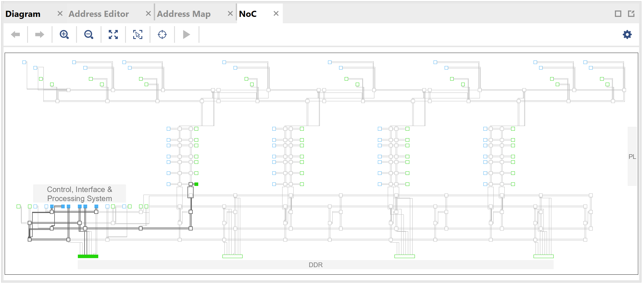
During the “Validate Design” process, the NoC Compiler is run. A new “NoC” tab will appear that will show a preliminary physical representation of the NoC resources used and their locations. These resources can be clicked on to get NoC Site Properties information. These locations are preliminary since Vivado can move these sites when the NoC Compiler is run during the placer implementation stage.
-
Also note a “NoC QoS” tab will appear that will detail NoC Traffic Class and required and estimated Bandwidth and Latency:
In this section, an HDL wrapper will be generated for the IP integrator Block Design, constraints will then be added to the project and the design synthesized. After it is synthesized, the Advanced IO Planner can be invoked to assign pins for the DDR-MC.
-
In the “Sources” tab, right click on the Block Design “design_1” and select “Create HDL Wrapper”. When the window pops up, keep the default and select “OK”.
-
Add the constraints file “constraints.xdc” that was provided with the tutorial to the project. This file contains initial clock and IO constraints for the PL logic. Later, additional DDR4 pin-out constraints will be defined and appended to this file.
-
Select “Flow Navigator > Project Manager > Add Sources”
-
Next select “Add or Create Constraints” then click on “Next”
-
Click on “Add Files” and navigate to the “/constraints/constraints.xdc” file provided with this tutorial.
-
Click on “Copy constraints files into project” and click on “Finish”
-
-
Next, Synthesize the design.
-
In the “Flow Navigator” pane, click on “Synthesis > Run Synthesis” and accept the default settings and click on “OK” to invoke synthesis or alternatively, click on the “Design Runs” tab and right click on “synth_1” and click “Launch Runs” and then “OK”.
-
The generation of IP output products and synthesis process can take ~1 hour to complete.
-
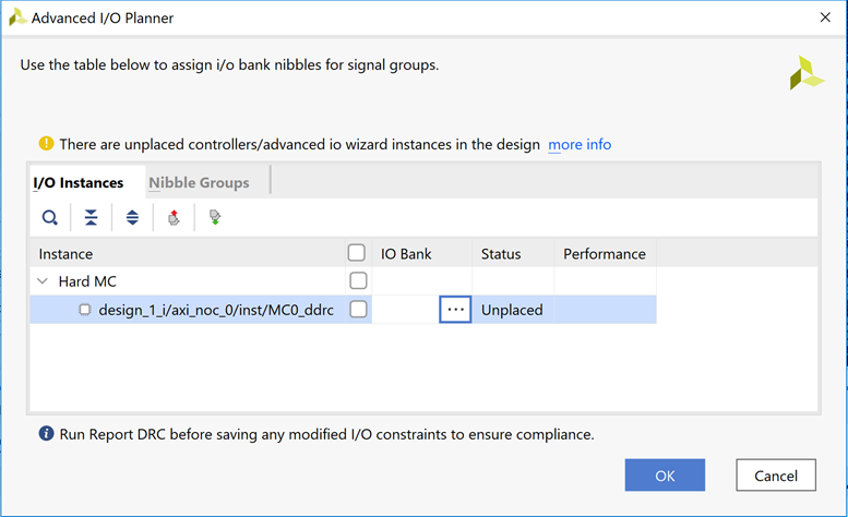
In this section, the “Advanced I/O Planner” will be used to assign a pin-out for the DDR-MC.
-
When the “Synthesis Completed” pop-up window appears, click on “Open Synthesized Design” and then click on “OK” open the Synthesized design in Vivado
-
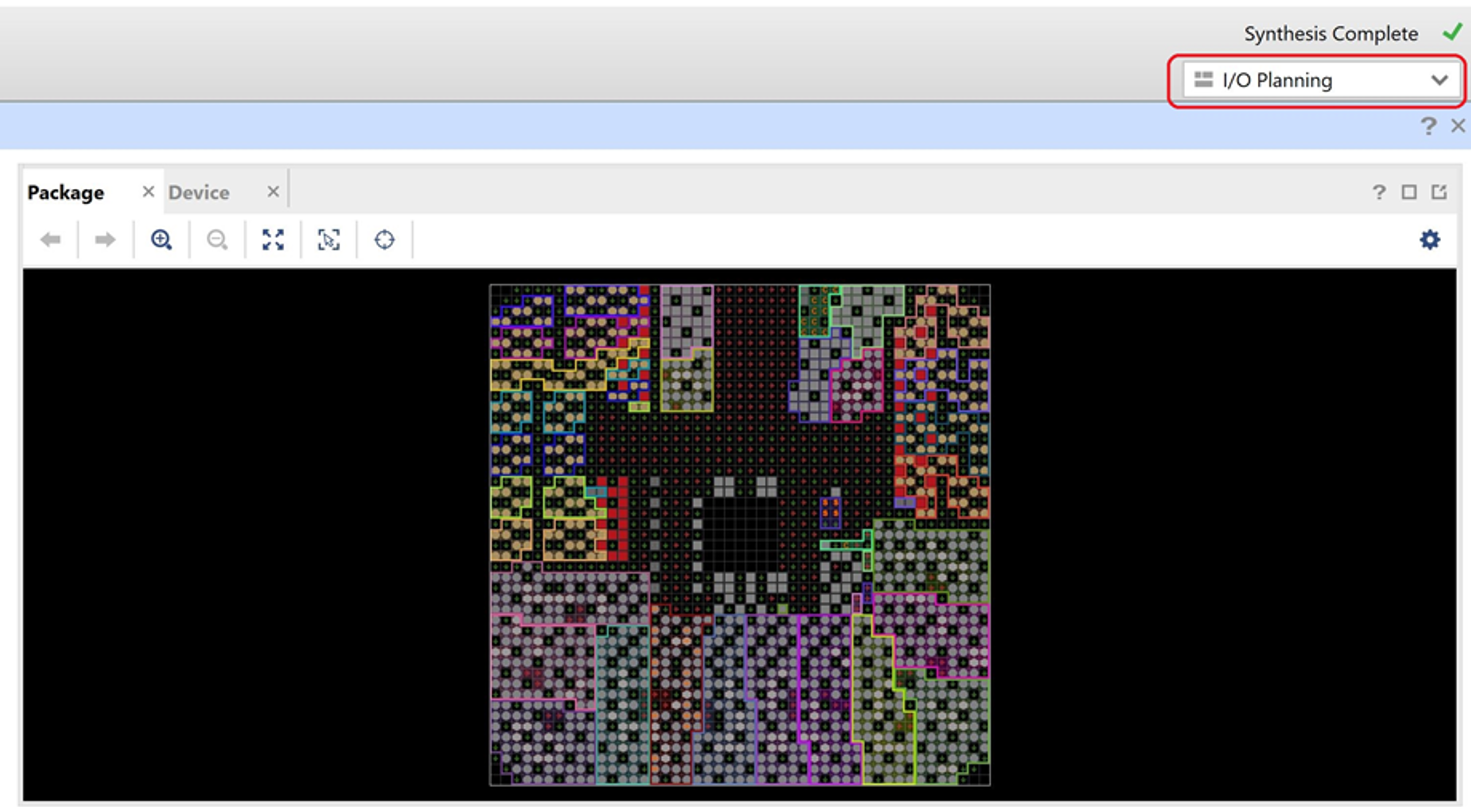
The Vivado layout view should be changed from “Default Layout” to “I/O Planning”. There is a pull-down menu for the layout view in the top right of Vivado as shown circled in red below:
-
In the I/O Ports tab, click on Open Advanced I/O Planner.
-
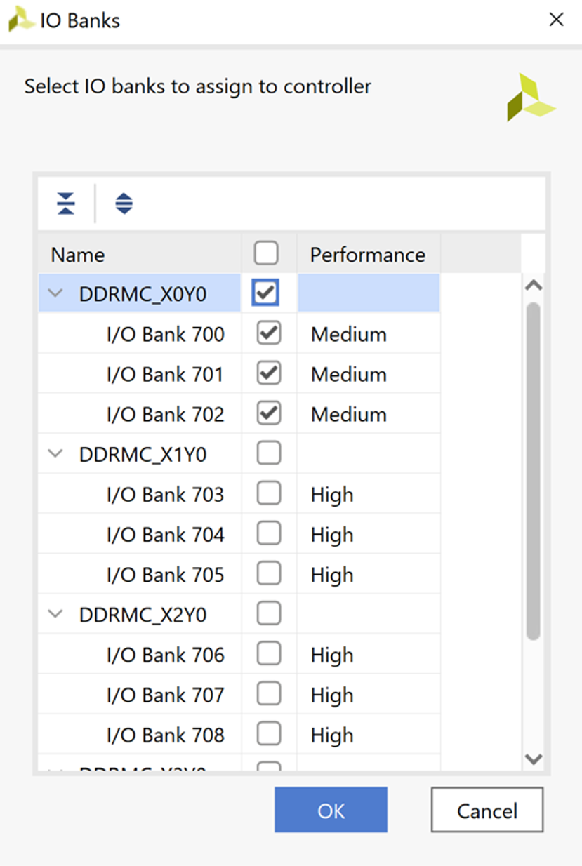
When the Advanced I/O Planner window pops up, click on the 3-dots in the IO Bank column. Then check the box next to DDRMC_X0Y0 to specifically select the DDR-MC location at X0Y0. This will automatically select the IO Triplet Banks of 700, 701, 702 and the pins for these banks. Select OK to exit the Advanced I/O Planner.
-
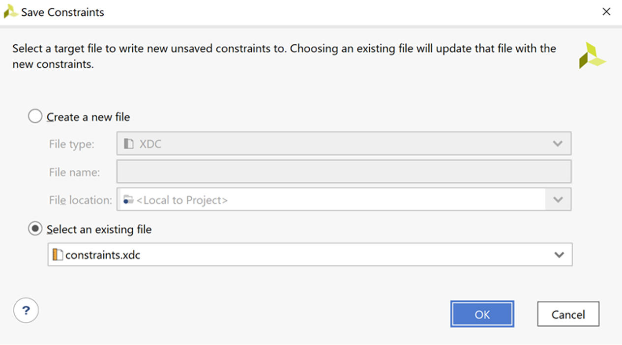
Save the new generated pin constraints to target constraints file “constraints.xdc”.
-
Select “File > Constraints > Save”
-
Verify “Select an existing file” selected and “constraints.xdc” is selected and then click on “OK”.
-
You will get a notification for an out-of-date design because the new constraints have been saved. This means that synthesis will have to be run again. Click OK.
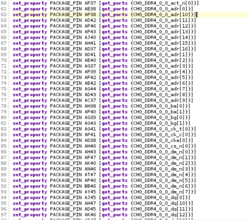
- The constraints.xdc file can be opened to verify that the constraints were generated and saved properly. Pinouts for ports beginning with the name “ddr4…” can be observed constrained to package pins as shown in this constraints file excerpt:
-
-
In the Vivado Flow Navigator pane, click Program and Debug --> Generate Device Image and click-through the following pop-up windows to generate the final implementation and device image.
-
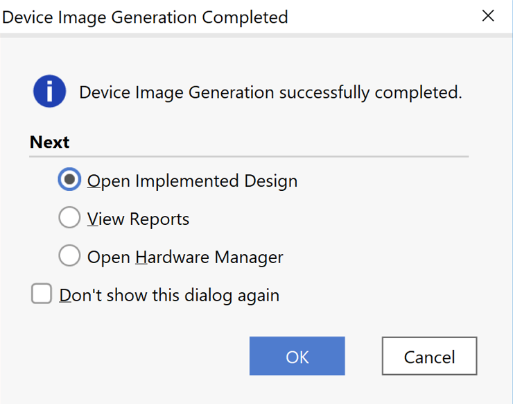
Once the device image is generated, the following pop-up window should appear. Click Cancel. This completes the tutorial.
Note: The device image file (.pdi) is now generated and can be found in the project runs sub-directory called “/impl_1”.
Copyright © 2020–2024 Advanced Micro Devices, Inc.
